English
 中文简体
中文简体7/16(L29) Micro-strip RF Connectors Manufacturer
Product Overview
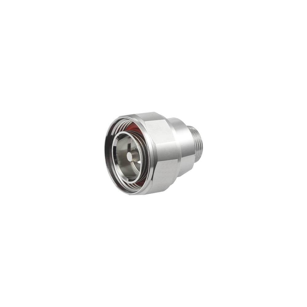
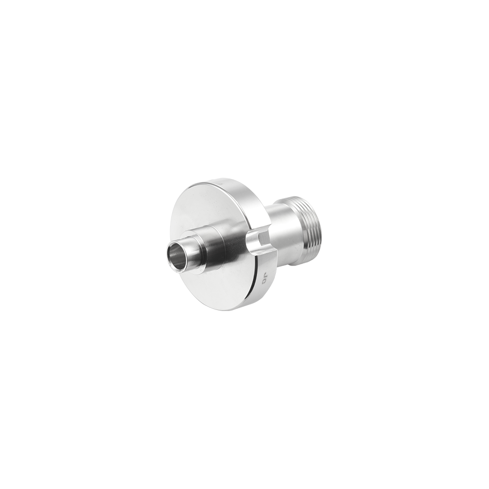
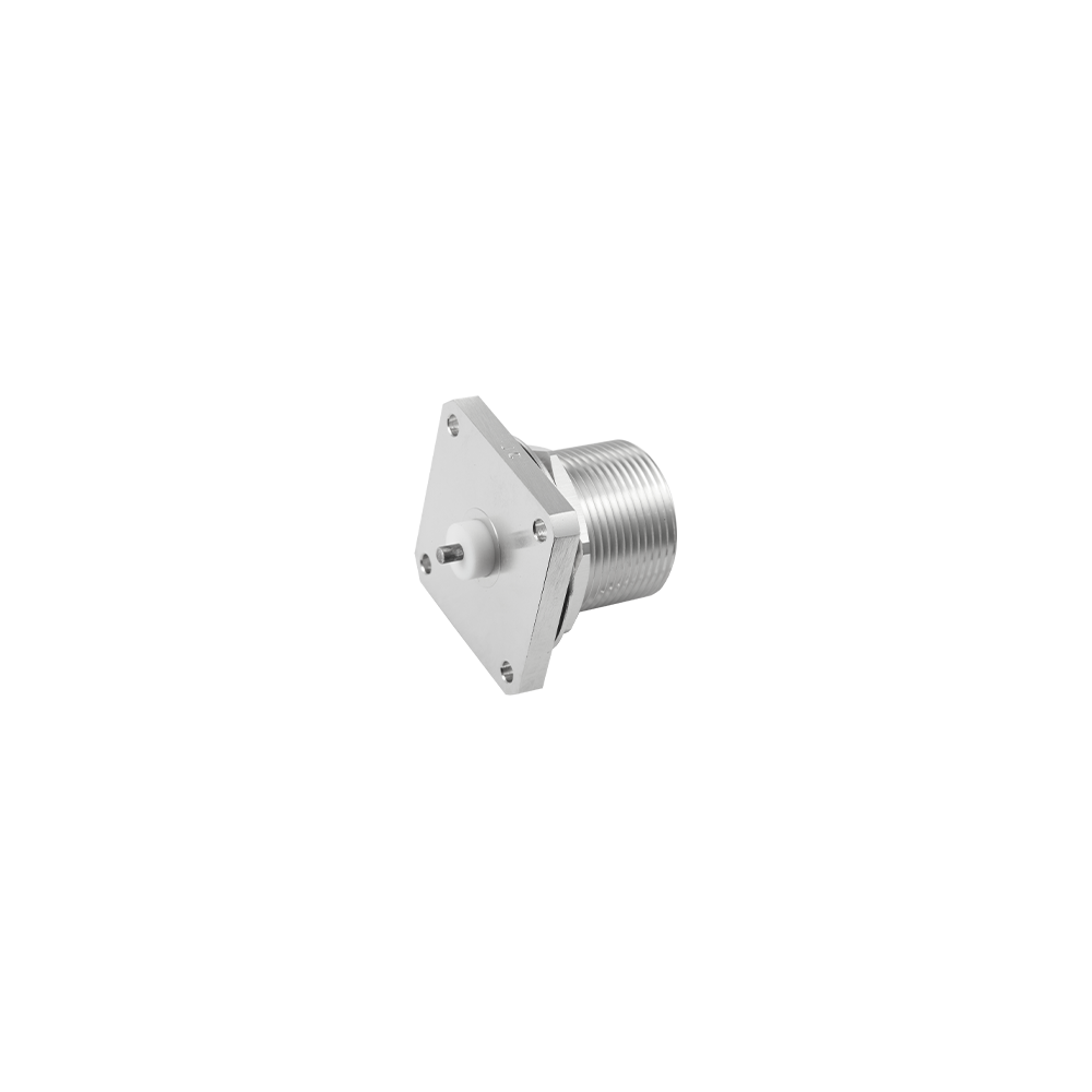
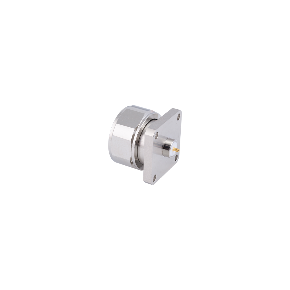
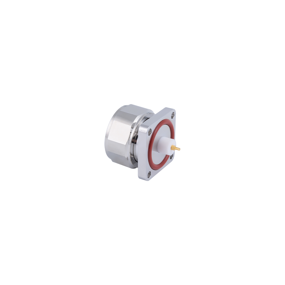
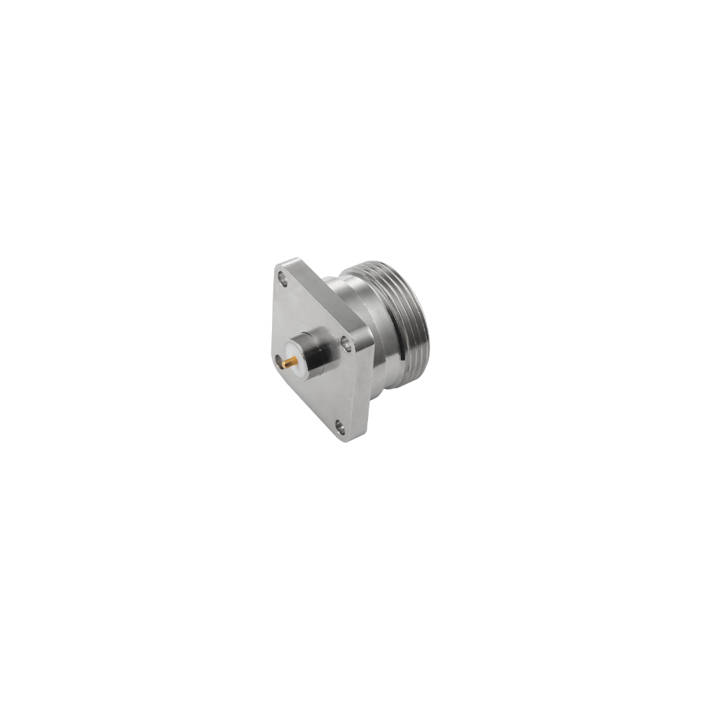
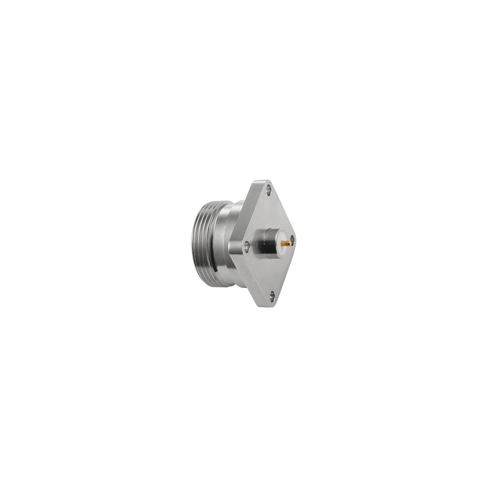
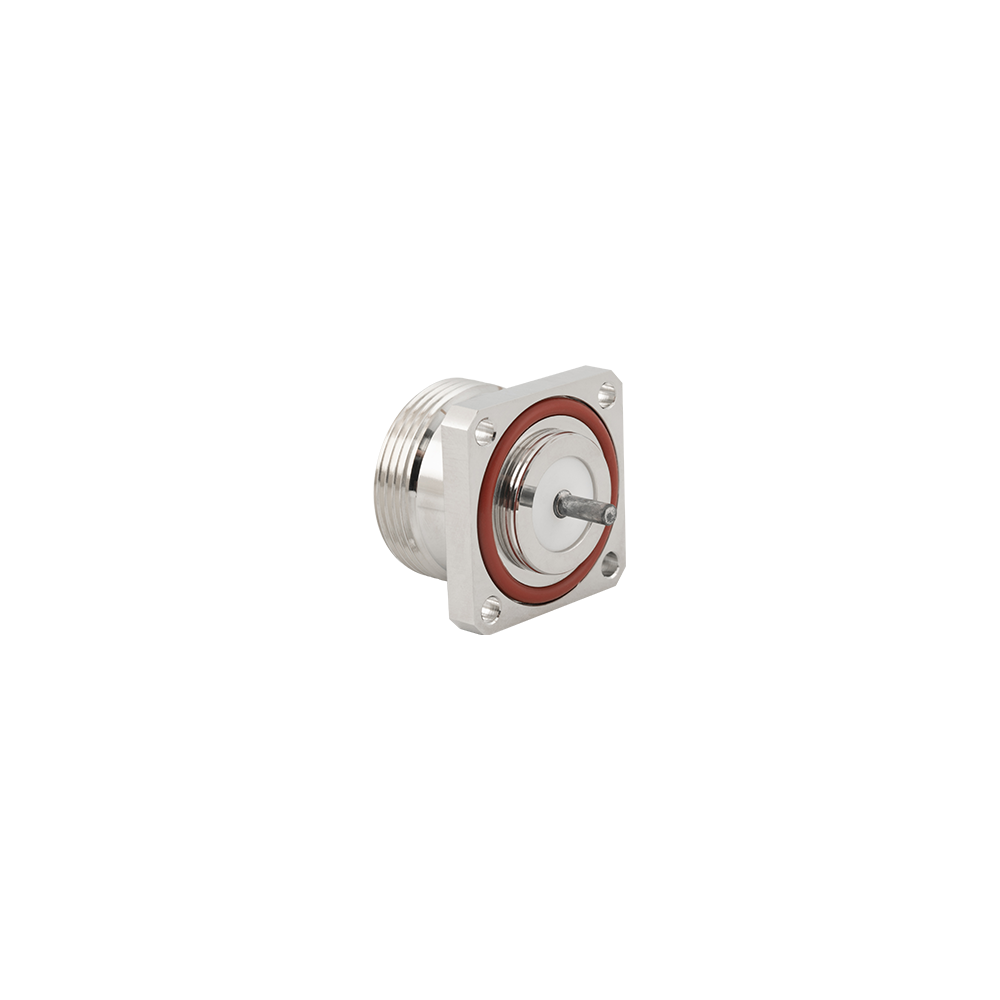
Integrating high-power RF amplification, signal combining, and power monitoring onto microwave PCB substrates requires 7/16 DIN connectors that launch directly from a PCB transmission line. This 7/16 micro-strip RF connector series bridges the transition between planar PCB transmission structures (microstrip, stripline, and suspended substrate configurations) and the 7/16 DIN coaxial interface. It enables PCB-based high-power module designs to connect directly to 7/16 DIN feeder infrastructure without an intervening adapter, minimizing insertion loss and passive intermodulation (PIM) at the board-to-connector transition.
Key Features
PCB edge-launch geometry optimized for smooth impedance transition from 50 Ω transmission lines to the 7/16 DIN coaxial interface, minimizing return loss.
Precision pin height and board alignment features minimize electrical impacts caused by alignment errors at the larger physical scale of the 7/16 format.
High-power-compatible dielectric materials and contact geometries manage the elevated voltage and current levels present in transmitter board applications.
Multiple soldering and mechanical fastening options provide secure board retention under vibration and thermal cycling.
Low-PIM design at the PCB interface incorporates optimized contact surfaces and material selections to minimize passive intermodulation.
Gold-plated center contact and controlled silver-plated outer conductor ensure optimal conductivity and solderability on the PCB attachment side.
Compatible with standard PCB thickness ranges used in broadcast and infrastructure communication module designs.
Mating interface conforms to standard dimensions, ensuring interoperability with all standard 7/16 DIN mating hardware.
Competitive Advantages
RF Engineering Capabilities: In-house RF engineering resources design and simulate connector transition geometries before tooling, reducing performance risks.
High-Power PCB Launch Specialization: Engineered specifically for high-power broadcast and communication applications, accounting for dielectric heating, thermal management, and PIM mechanisms.
Simulation-Backed Design: Transition geometries are validated using electromagnetic simulation before production tooling to ensure performance targets are met without project delays.
Prototype-to-Production Pipeline: In-house tooling capabilities support fast prototype turnaround followed by volume production scale-up for new board designs.
Application Engineering Support: Technical support is available to review PCB parameters and layout configurations to recommend the correct connector footprint for specific module designs.
Typical Applications
Solid-state broadcast transmitter final amplifier stage PCB output ports
High-power RF combiner and splitter PCB module connector ports in broadcast systems
Transmitter solid-state amplifier module PCB RF output interfaces
Phased-array systems and communication module PCB connector interfaces
Satellite uplink power amplifier driver stage PCB assemblies
High-power RF test fixture PCB signal injection and extraction points
Base station and communication transmitter module PCB connector ports
FAQ
Q: At what power levels are your 7/16 micro-strip PCB connectors rated?
A: The power handling of a PCB-mount connector depends on the PCB substrate, trace geometry, ambient temperature, and frequency. We design our 7/16 micro-strip connectors for the elevated power levels associated with broadcast and radar PCB module applications.
Q: What PCB substrate materials are your 7/16 micro-strip connectors compatible with?
A: Our 7/16 micro-strip connectors are designed for use on PCB substrates including low-loss PTFE-based laminates, ceramic-filled hydrocarbon laminates (such as Rogers RO4000 and RO3000 series), and other substrates commonly used in broadcast and radar amplifier modules.
Q: Can you supply a PCB footprint and recommended layout guidelines for your 7/16 micro-strip connector?
A: Yes. We provide a recommended PCB footprint, land pattern, and solder process guidelines with each connector model. For new high-power module designs, our application engineering team is available to review your PCB layout and suggest transition geometry optimizations before you commit to PCB fabrication.