English
 中文简体
中文简体4.1-9.5 Micro-strip RF Connectors Manufacturer
Product Overview
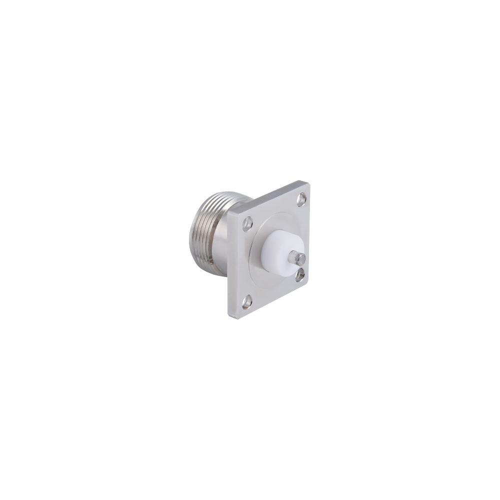
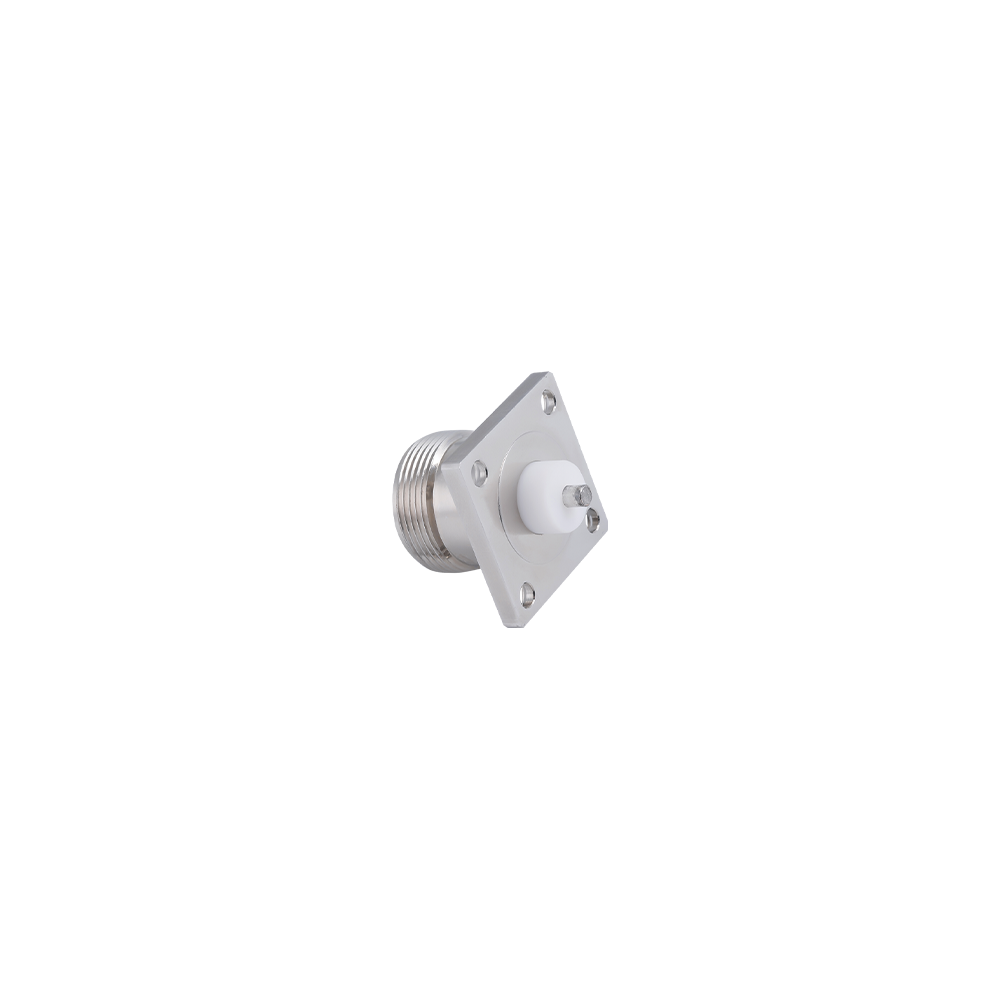
PCB integration and microwave substrates require RF connectors that launch signals from planar transmission lines (microstrip, stripline, or coplanar waveguide) directly to a coaxial port with minimal discontinuity, radiation loss, or impedance mismatch. This 4.1-9.5 micro-strip RF connector series provides a PCB launch design that enables a smooth transition from the PCB transmission line to the 4.1-9.5 coaxial interface. These connectors support edge-launch and surface-mount configurations, available with integrated PCB mounting hardware such as soldering tabs, PCB posts, or flange designs that align the connector center pin to the board trace during assembly.
Key Features
Optimized coax-to-microstrip transition geometry to minimize return loss and insertion loss across DC to 6 GHz.
Edge-launch and surface-mount (vertical) configurations for PCB layout flexibility.
Center pin geometry matched to standard 50 Ω microstrip trace widths on common PCB substrates including standard FR4 laminates.
Precision-controlled pin height and board alignment features to standardize PCB assembly and reduce solder joint variability.
Low-profile body design minimizing PCB footprint area for dense multi-port antenna arrays and module designs.
Gold-plated center pin and contact surfaces for reliable solderability and long-term low contact resistance.
Through-hole and SMT mounting flange options for compatibility with automated PCB assembly lines.
Compatible with automated wave solder and selective solder processes when appropriate through-hole versions are specified.
Competitive Advantages
RF Engineering Expertise: In-house RF engineering capabilities design and simulate connector transition geometries before tooling, reducing development risks.
Precision Machining for PCB Launch: Center pin height and alignment are maintained to precise tolerances using CNC machining lines to ensure consistency across production batches.
Substrate Compatibility: Compatible with standard FR4 and composite substrates, supporting footprint optimization for specific substrate and trace geometries.
Test and Verification: All micro-strip connector designs are characterized on VNA platforms to produce measured S-parameter data for system-level simulation.
Prototype Support: Factory supports small-quantity prototype runs to allow verification of the connector-to-PCB interface before final production tooling.
Typical Applications
Active antenna unit (AAU) and massive MIMO array PCB signal ports
Phased array systems and electronic communication module RF input/output ports
Microwave transceiver module and amplifier board RF ports
Signal conditioning and RF distribution PCB assemblies in base station baseband units (BBU)
Satellite communication modem and outdoor unit (ODU) board RF interfaces
RF test fixture PCB ports for automated test equipment (ATE) environments
Commercial vehicle communication module board connectors
FAQ
Q: Can you provide a recommended PCB footprint and land pattern for your micro-strip 4.1-9.5 connectors?
A: Yes. A recommended PCB footprint, land pattern, and soldering guidelines are provided with each connector product. Footprint optimization reviews are available based on provided Gerber files.
Q: What PCB substrates have your micro-strip connectors been validated on?
A: These connectors are used on standard FR4 and common network-layer substrates. Performance depends on the specific trace geometry and dielectric properties.
Q: Are your micro-strip 4.1-9.5 connectors suitable for automated PCB assembly using SMT pick-and-place?
A: Selected surface-mount versions of these micro-strip connectors are compatible with automated SMT pick-and-place assembly. Please specify the assembly method when requesting information.