English
 中文简体
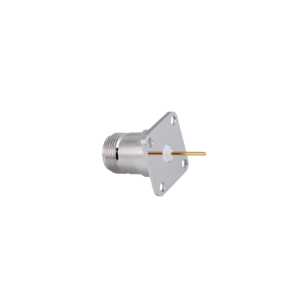
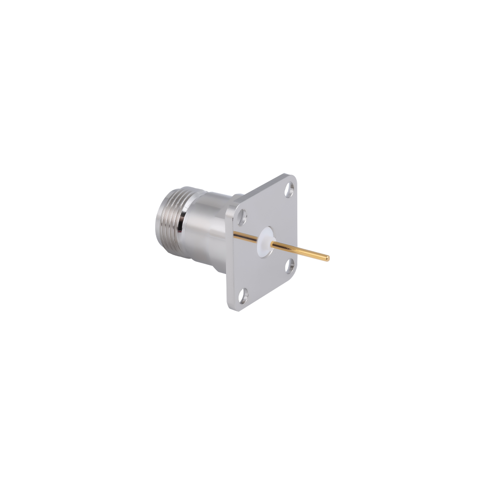
中文简体N Micro-strip RF Connectors Manufacturer
Product Overview
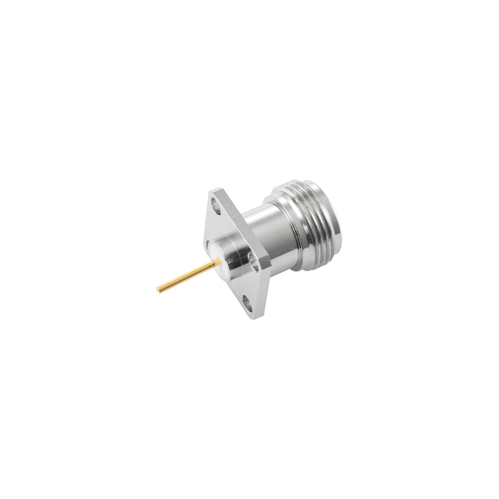
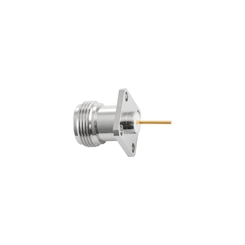
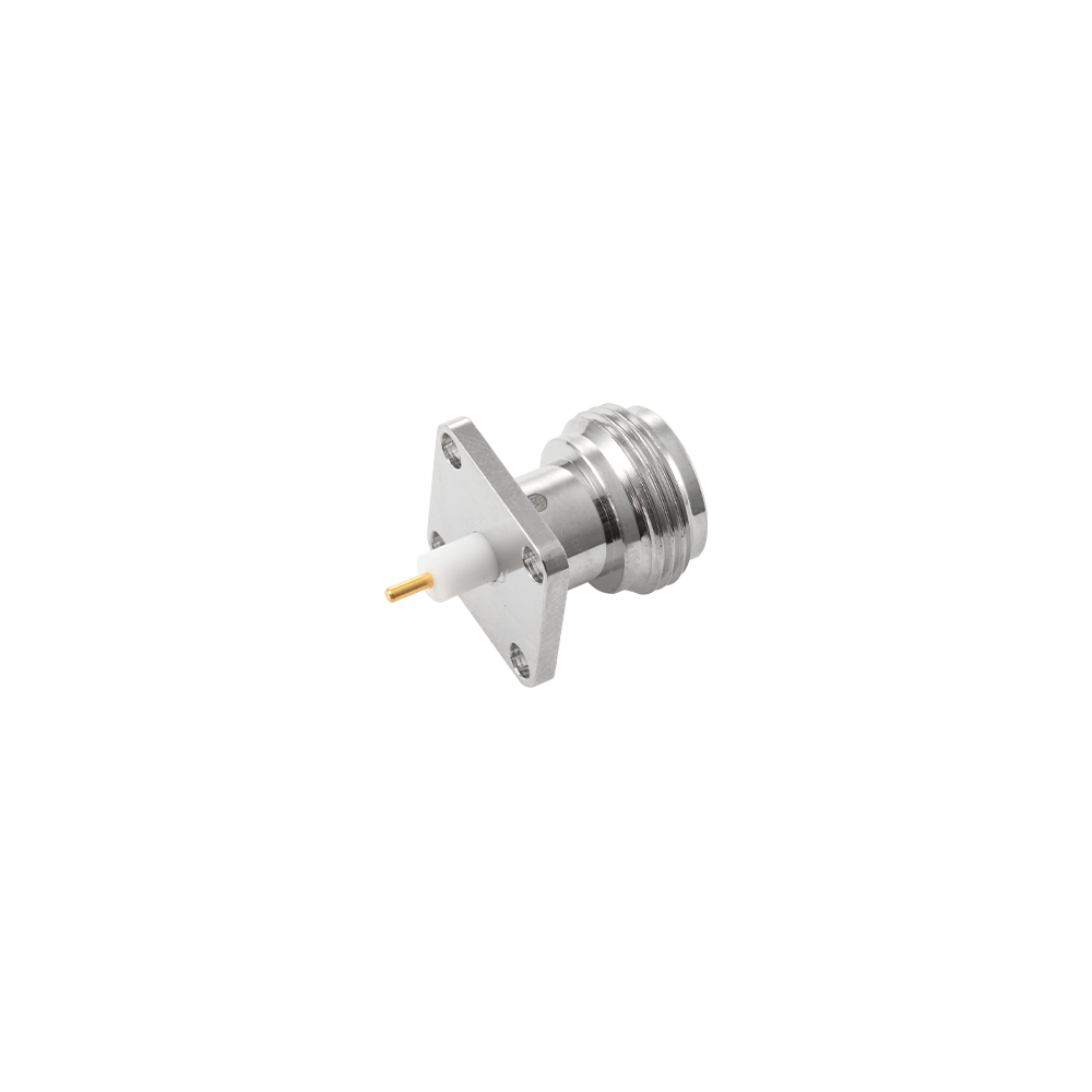
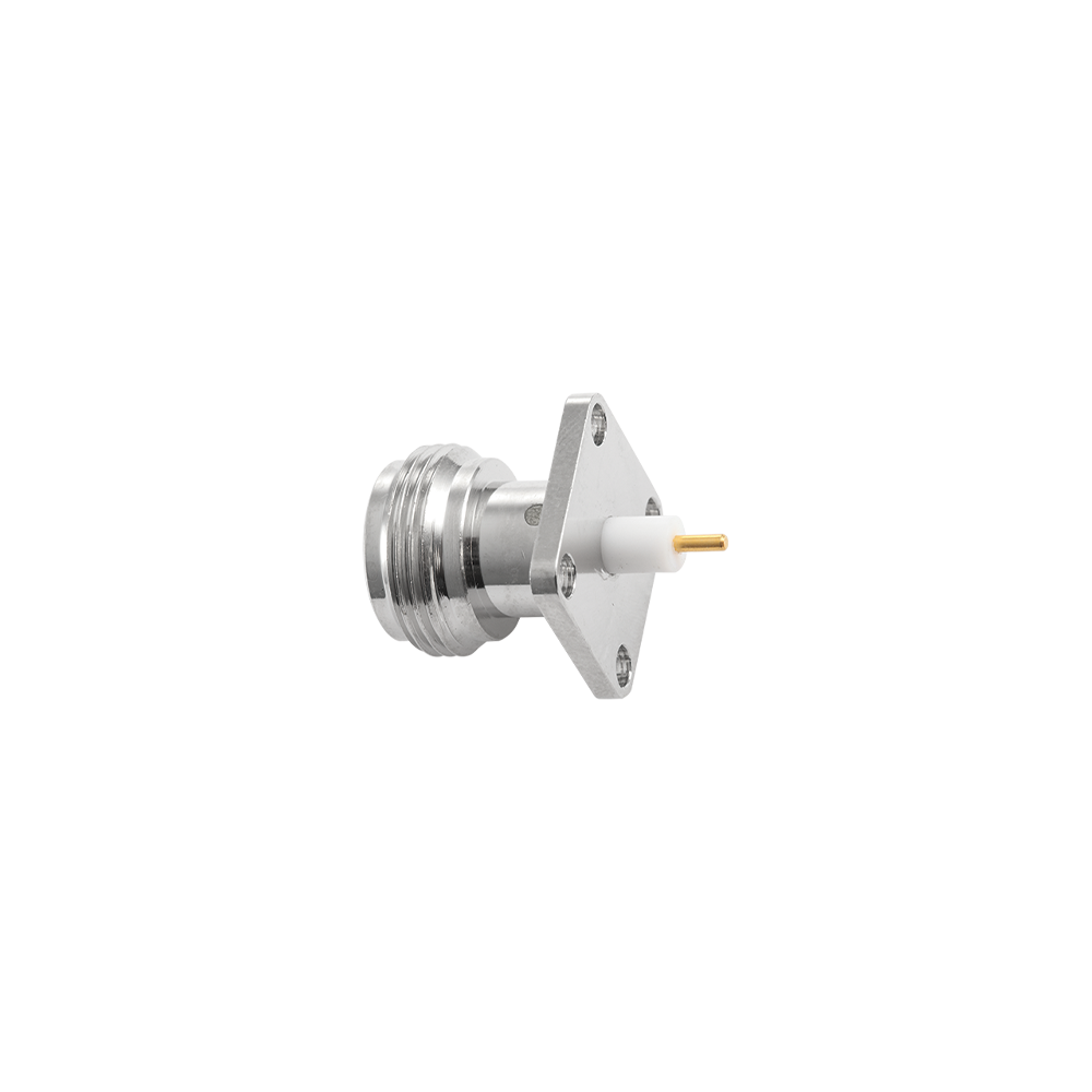
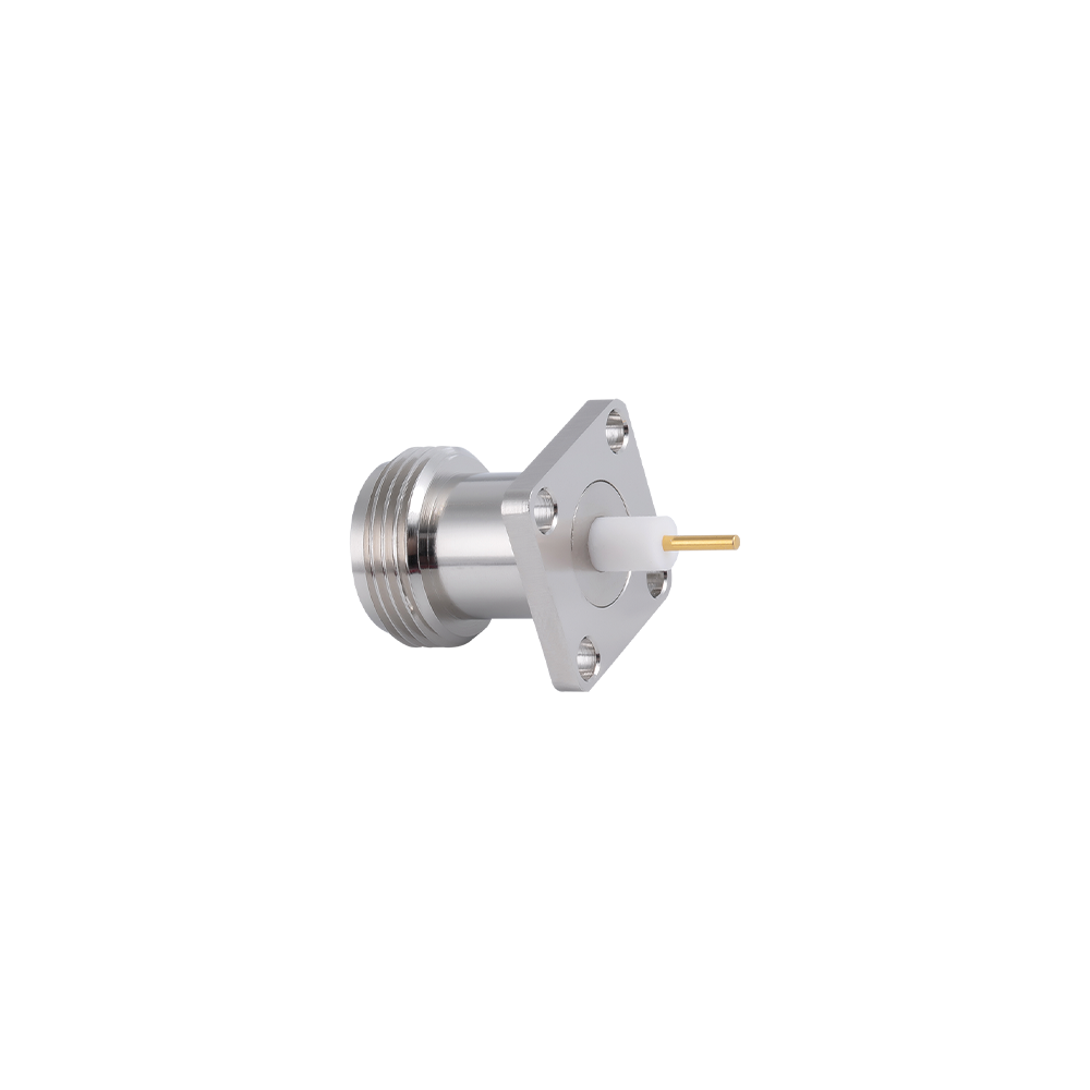
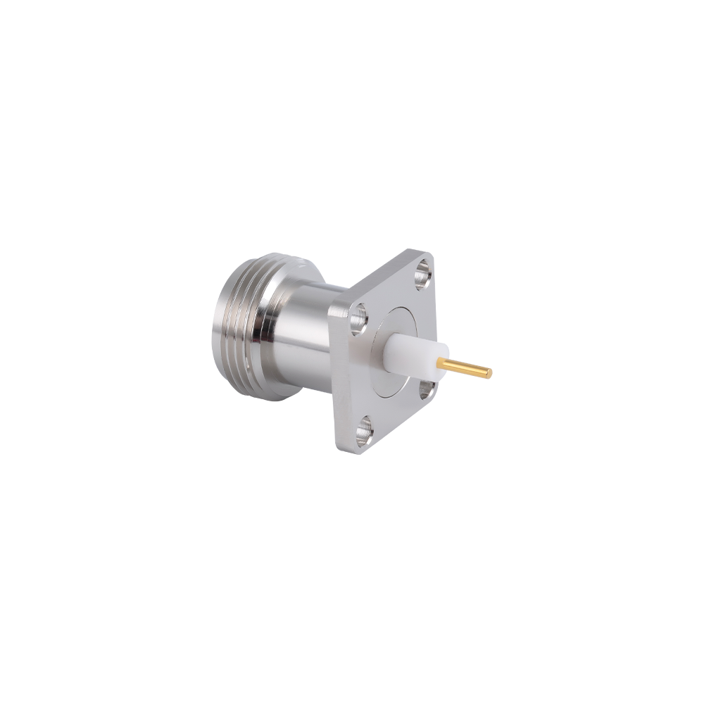
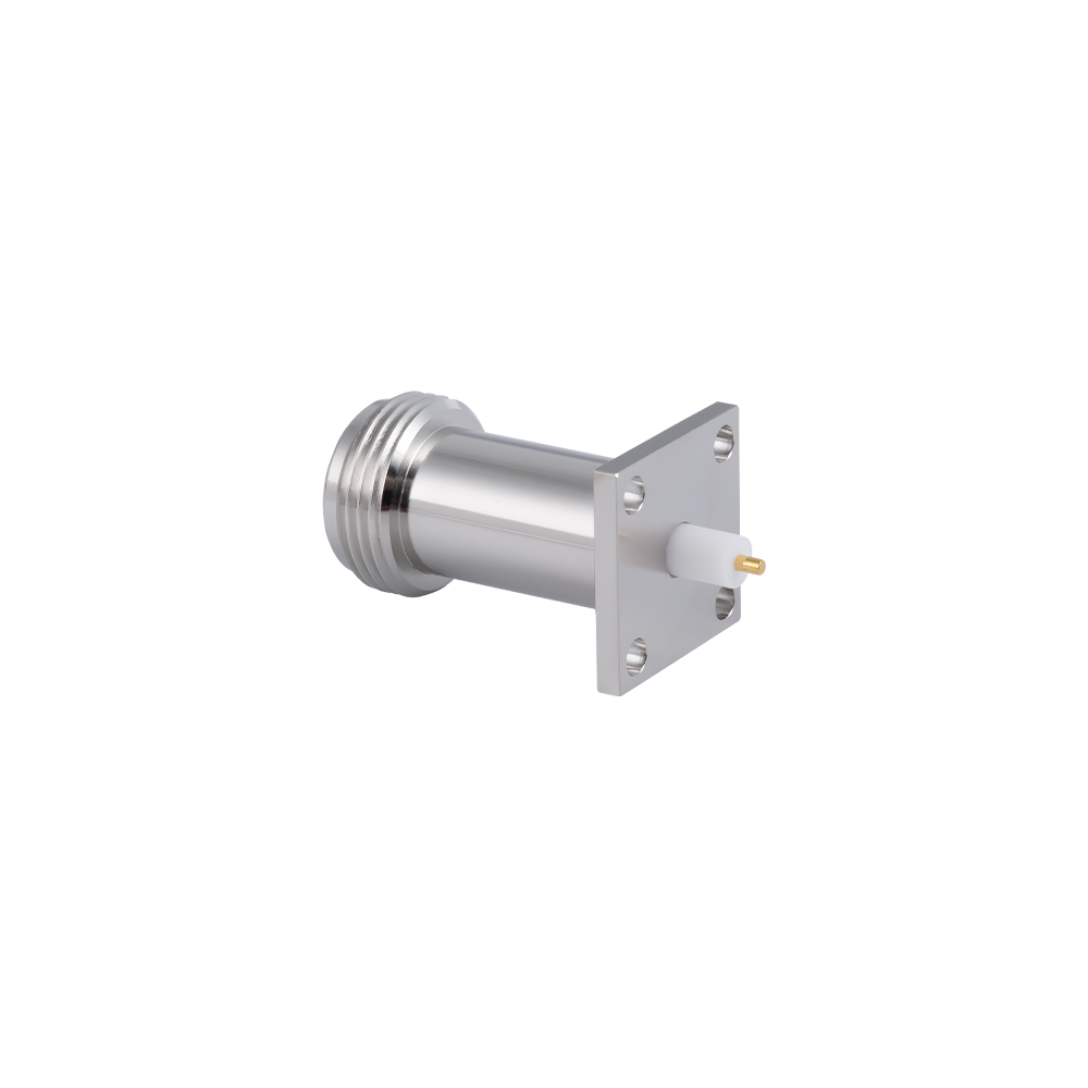
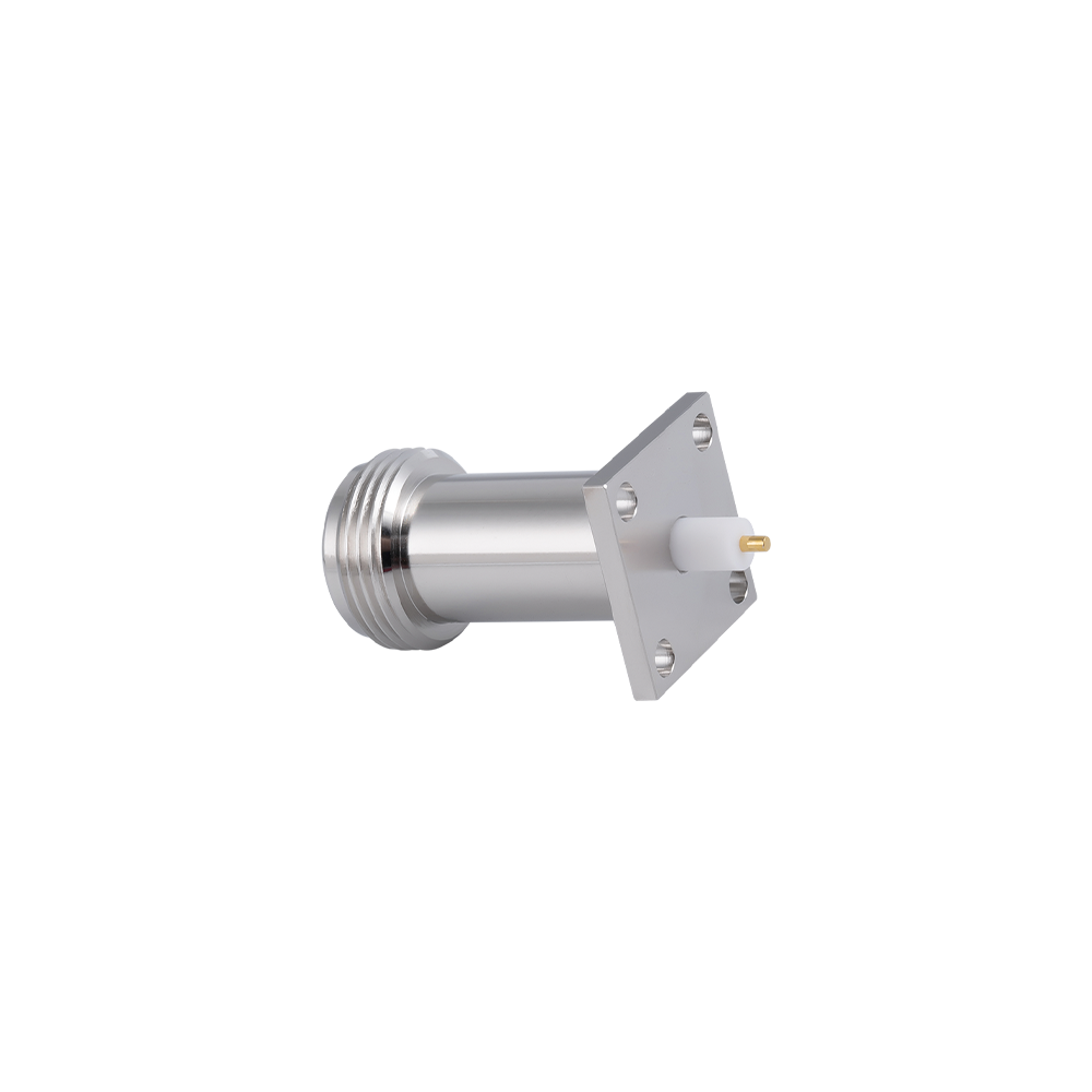
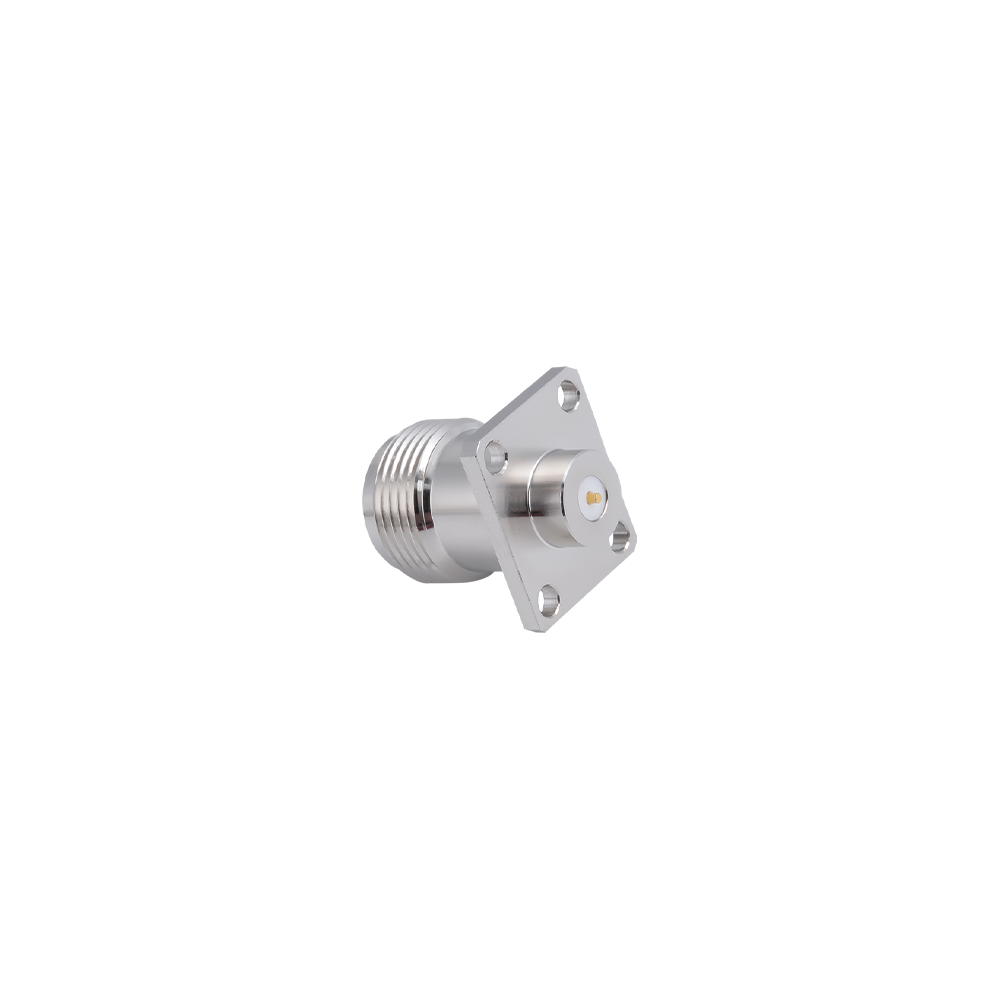
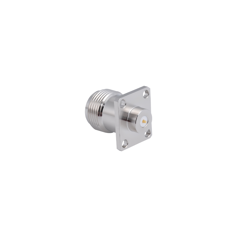
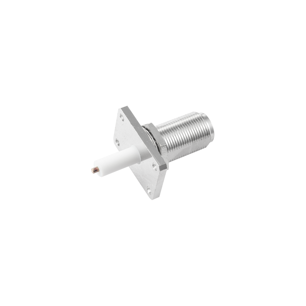
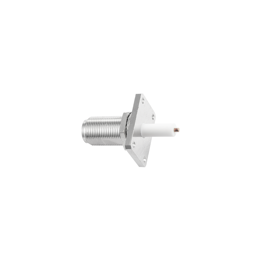
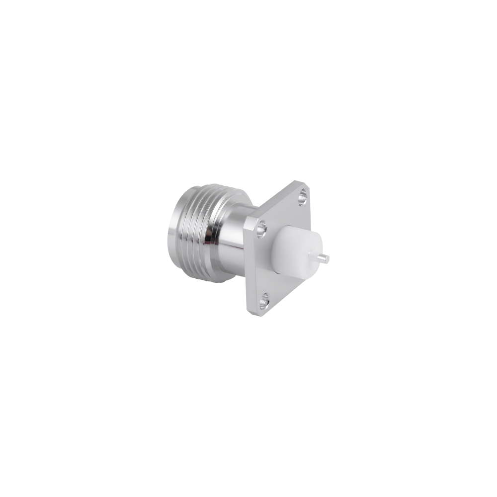
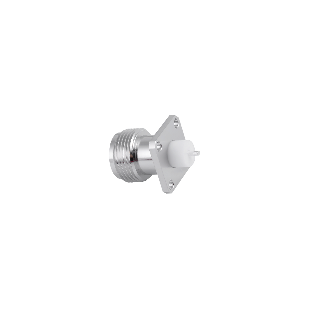
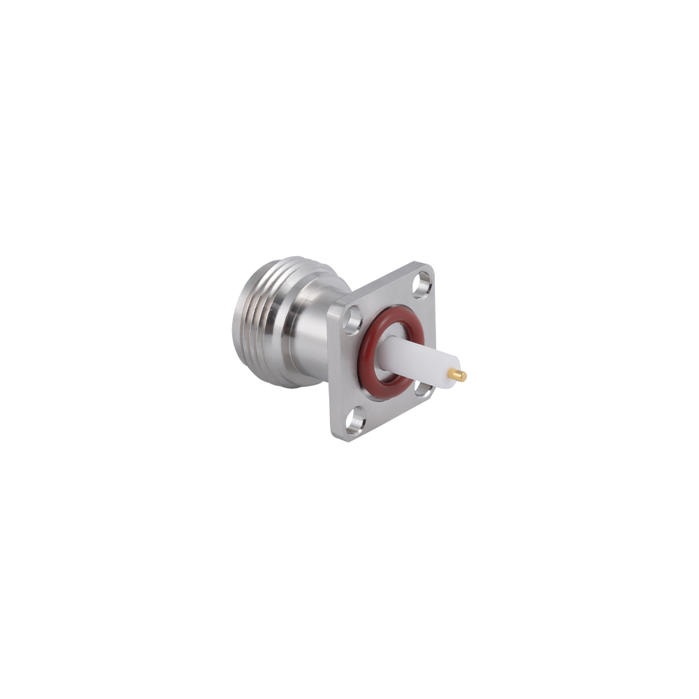
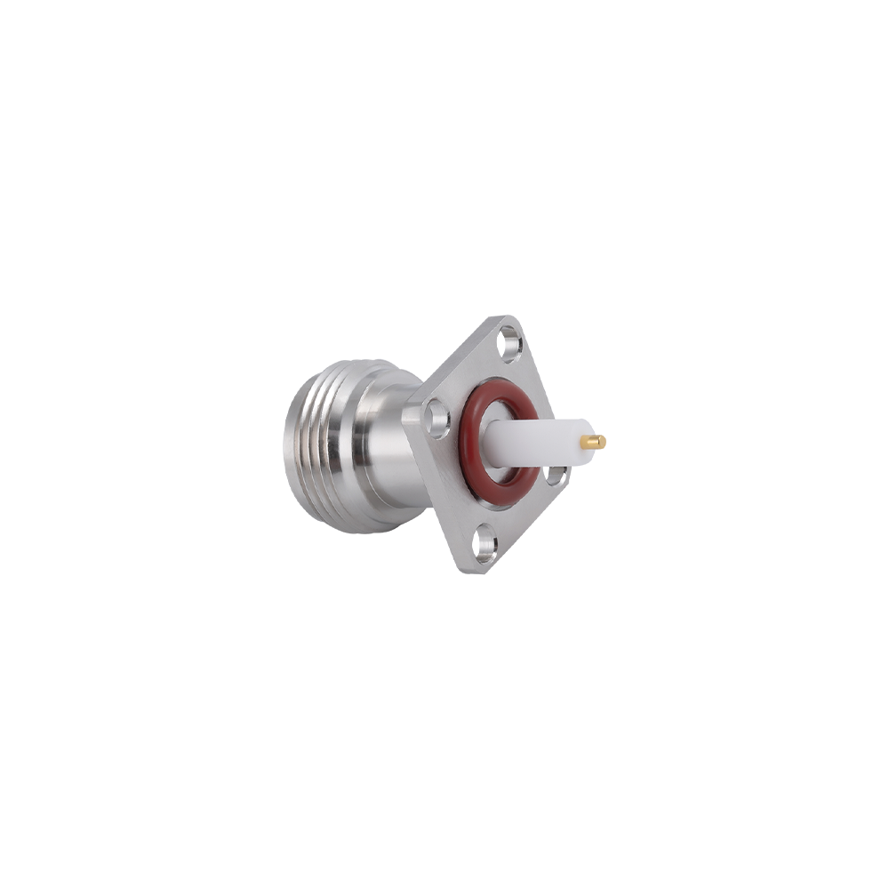
N-type Micro-strip RF Connectors are a specialized sub-family within the N series, designed specifically for direct electrical connection to microstrip transmission lines on PCBs and microwave substrate assemblies. Rather than terminating to a coaxial cable, the micro-strip connector interfaces directly with a planar transmission line structure—the center contact makes direct electrical contact with the microstrip signal trace, while the body grounds to the PCB ground plane through multiple grounding contacts or soldered feet.
This direct PCB-to-connector transition is used in microwave module assemblies, filter and amplifier test fixtures, phased-array antenna element feeds, and calibration standards where the traditional approach of using a separate PCB connector plus a cable pigtail to reach the N-type interface would add unacceptable insertion loss and calibration uncertainty. The micro-strip connector collapses the transition to a single, well-characterized interface that can be modeled in electromagnetic simulation and characterized by a single S-parameter measurement.
Key Features
Edge-launch (horizontal) and top-launch (vertical) contact configurations enable adaptation to both edge-mounted and center-board PCB integration scenarios.
Center contact geometry optimized for specific PCB substrate dielectric constants and microstrip line widths (commonly 50Ω characteristic impedance lines on Rogers, PTFE-glass, or FR4 substrates); custom contact profiles available for non-standard substrates.
Multiple ground contact feet or solder tabs provide low-inductance, symmetric grounding to the PCB ground plane—critical for suppressing connector-launch ground plane currents that cause resonances and spurious responses in microwave circuits.
Precision-machined PTFE or air-gap dielectric interface maintains insertion loss and return loss performance through the PCB transition zone at frequencies approaching the N-type series limit.
Operating frequency to 11 GHz; the micro-strip launch geometry limits the practical upper frequency more than the connector body itself, and Jingcheng's engineering team can advise on PCB layout optimization to extend usable frequency range.
Solder-down and press-fit (compression) mounting options; press-fit versions allow non-permanent installation for test fixtures that are frequently reconfigured.
Competitive Advantages
Jingcheng's in-house engineering R&D center has the electromagnetic simulation capability to model the micro-strip connector launch on customer PCB stackups and recommend geometry optimizations before physical prototypes are produced—a service level that smaller connector suppliers and trading companies cannot offer.
Custom center contact profiles for non-standard substrate widths are manufactured in-house on CNC turning centers without outsourcing, enabling rapid NPI turnaround when a customer's PCB design uses a non-standard trace impedance or substrate material.
Press-fit (contactless-solder) mounting versions provide a reusable connector installation for test fixture PCBs that must be re-used across multiple device-under-test generations without a new PCB being fabricated for each connector update.
Typical Applications
Microwave module and MMIC test fixture PCBs requiring direct N-type interface access
Phased-array antenna element feed network boards (space and defense applications)
Microwave filter, coupler, and power divider characterization test fixtures
Calibration standard assemblies for N-type VNA calibration kits
RF PCB development boards for wideband transceiver prototype characterization
FAQ
Q: What PCB substrate materials are supported for the micro-strip connector center contact geometry?
A: Standard contact profiles are available for the most common microwave substrate materials, including Rogers RO4003C, RO4350B, RT/duroid 5880, and standard FR4 (for applications below 3 GHz). For other materials (e.g., alumina, LTCC, or high-dielectric Rogers substrates), the center contact width must be custom-profiled to match the 50Ω trace width for that dielectric.
Q: How is the micro-strip connector grounded to the PCB?
A: Multiple solder-down grounding tabs on the connector body contact the PCB top-layer ground plane, which must be connected to the PCB back-side ground plane through a dense grid of through-hole vias immediately surrounding the connector footprint. The via fence design is critical: insufficient via density or incorrect spacing creates ground plane inductance that degrades connector return loss above 3 GHz. Jingcheng's application note on micro-strip connector PCB layout is available on request.
Q: Can press-fit micro-strip connectors be used on PCBs with conformal coating?
A: Press-fit connector mounting relies on contact pressure between the connector ground tabs and the PCB surface. Conformal coating on the landing area will electrically isolate the ground contacts, degrading RF performance. The connector landing area must be masked during conformal coating application. Please consult the conformal coating masking guidelines in the product application note.
|
Temperature Range |
-55~+155℃(PE Cable -40~+85℃) |
|
Impedance |
50Ω, 75Ω |
|
Frequency Range |
DC~11GHz |
|
Insulation resistance |
≥5000MΩ |
|
Insertion loss |
≤0.2dB(6GHz) |
|
VSWR |
Straight ≤1.15/6GHz |
|
Right angle |
≤1.25/6GHz |
|
Durability(mating) |
≥500 (cycles) |