English
 中文简体
中文简体BNC PCB Connectors Manufacturer
Product Overview
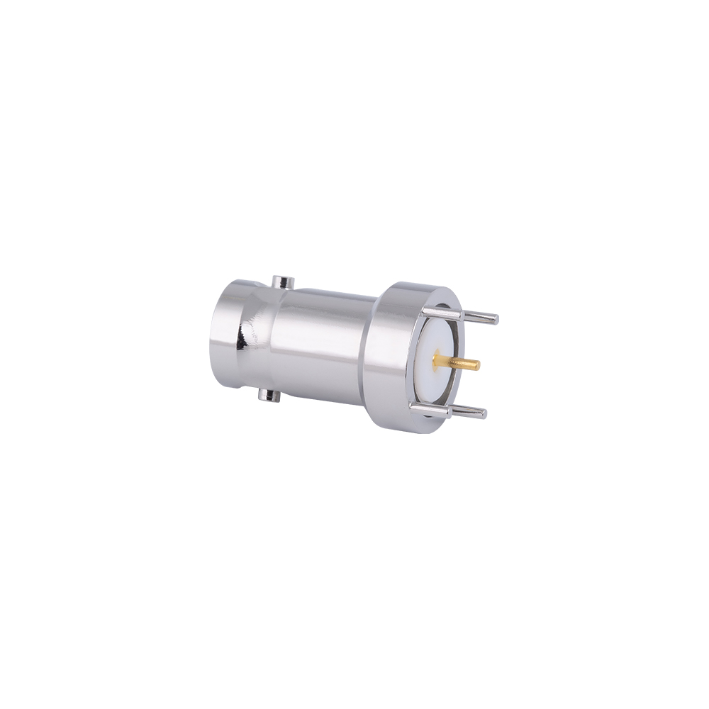
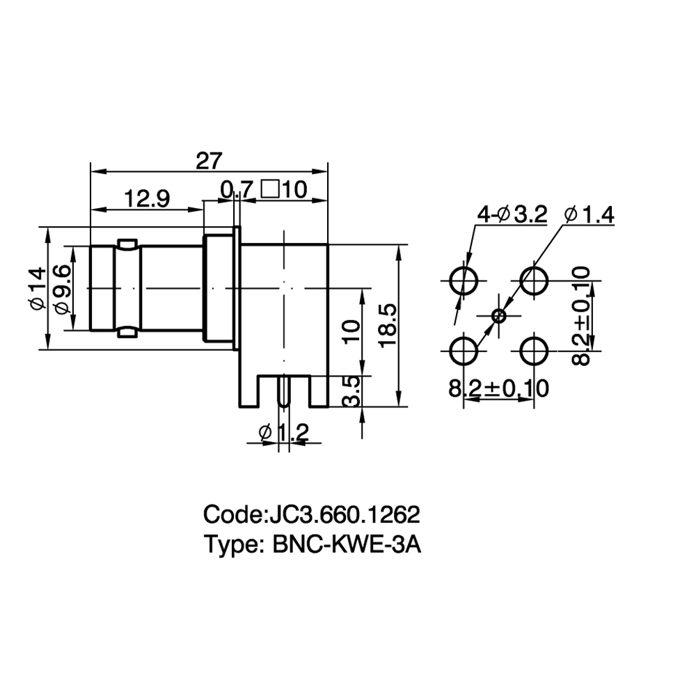
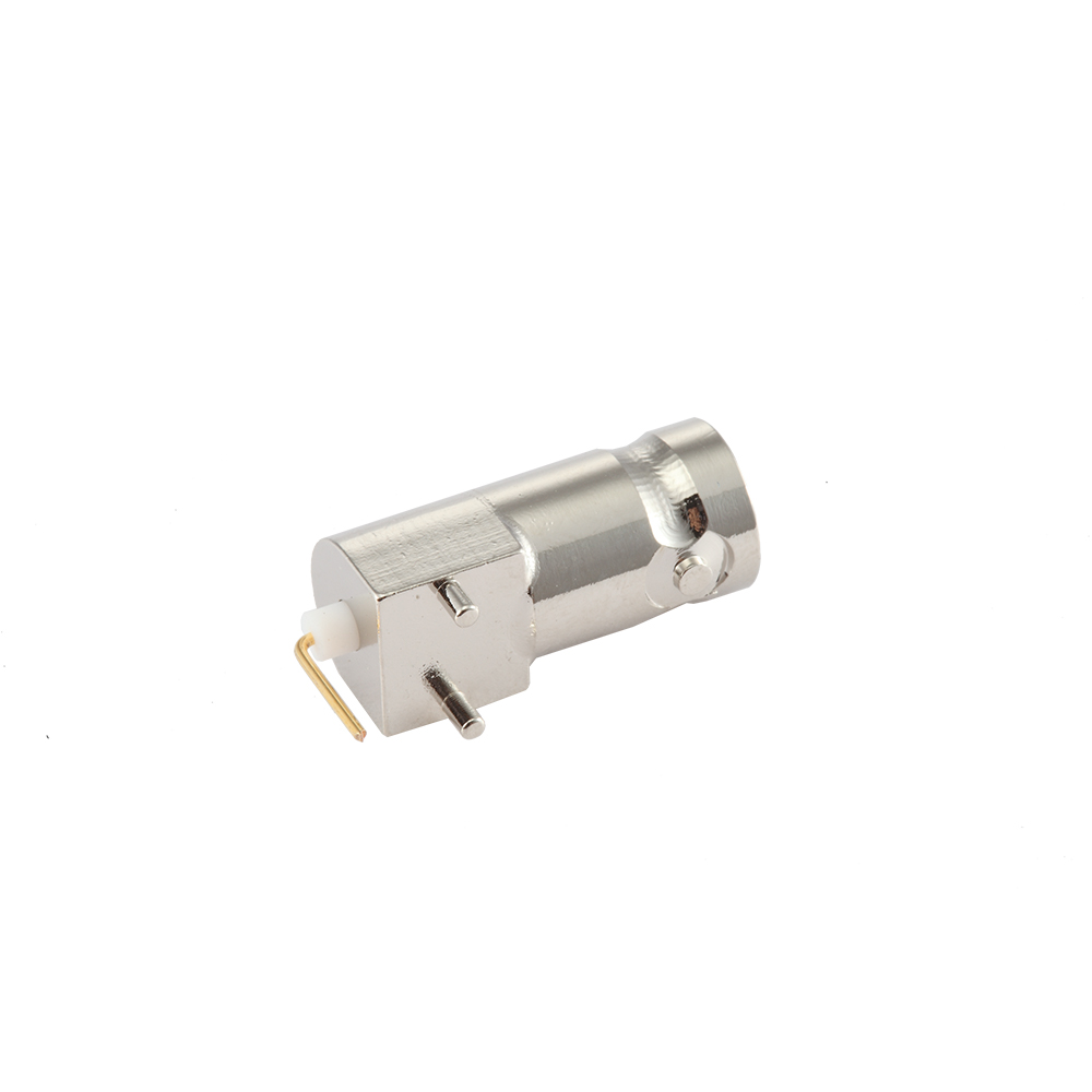
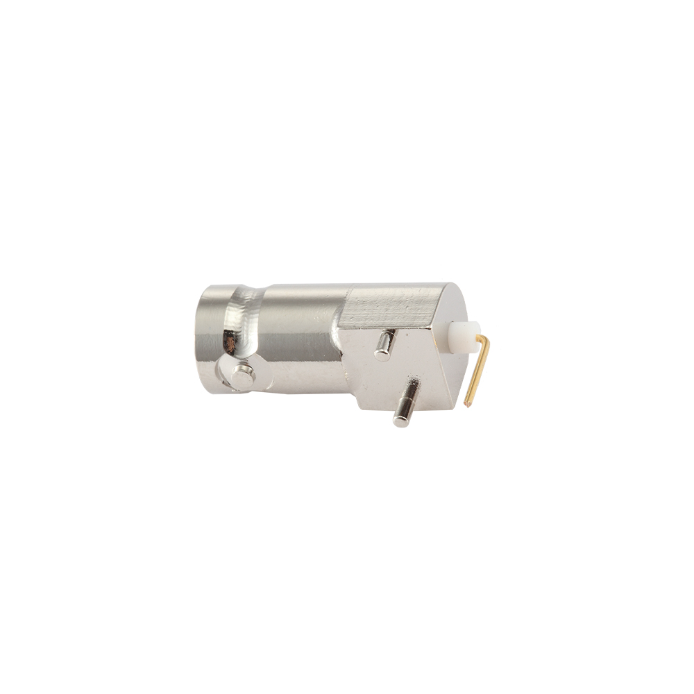
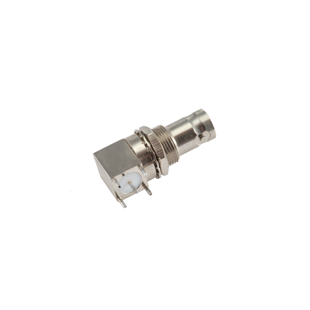
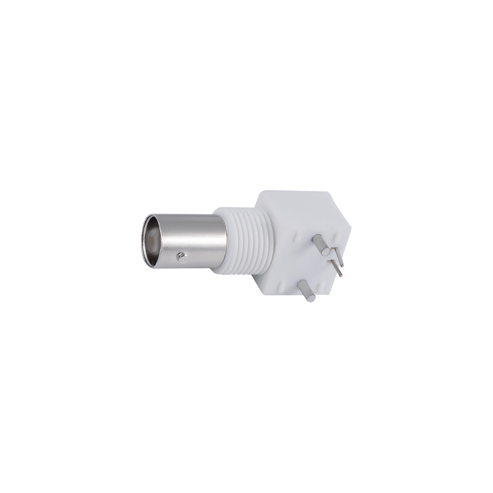
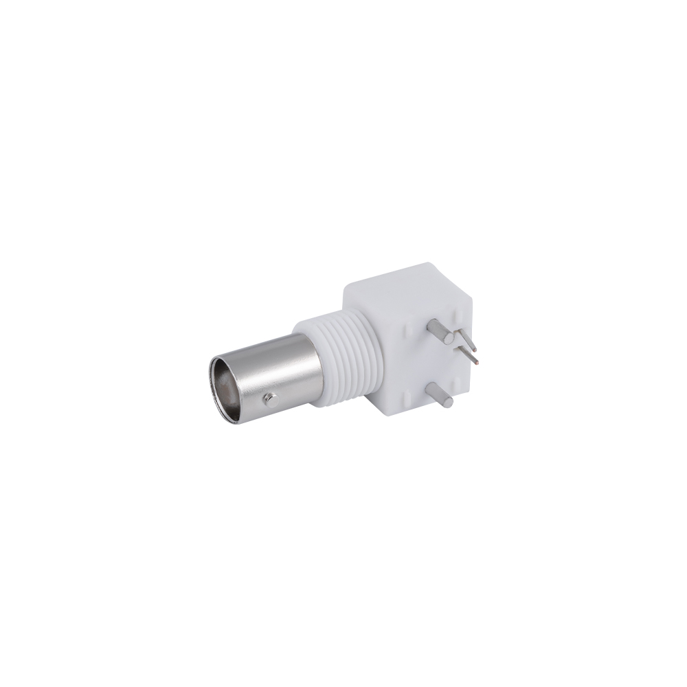
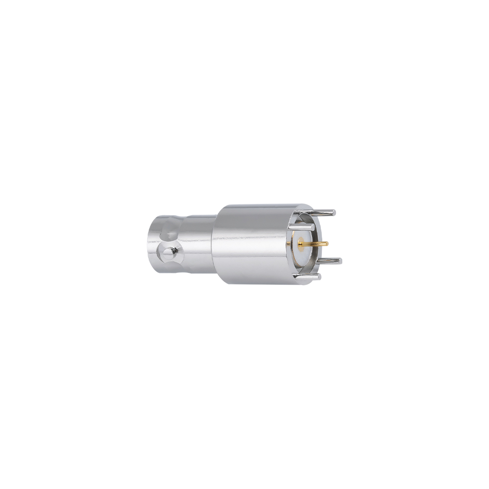
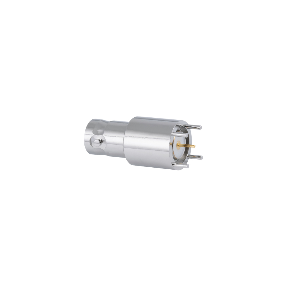
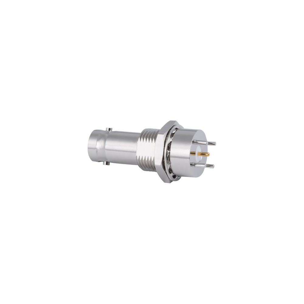
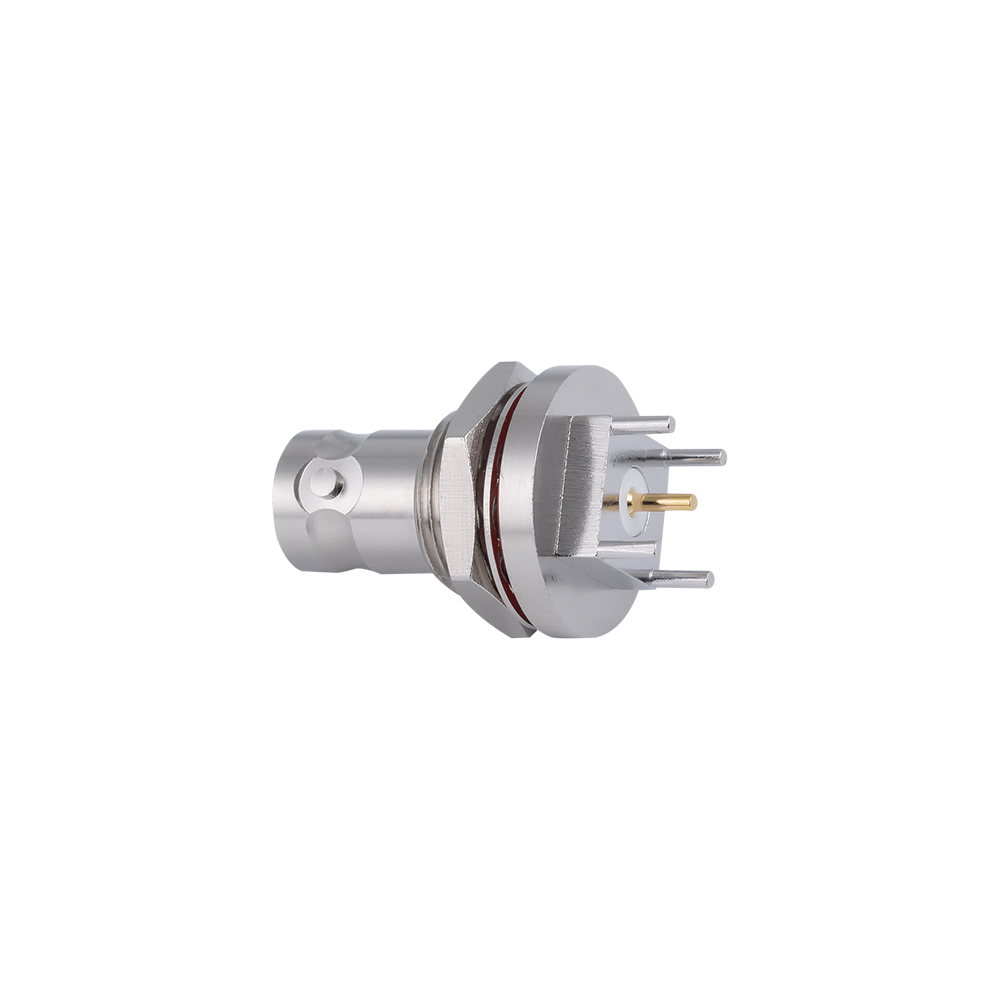
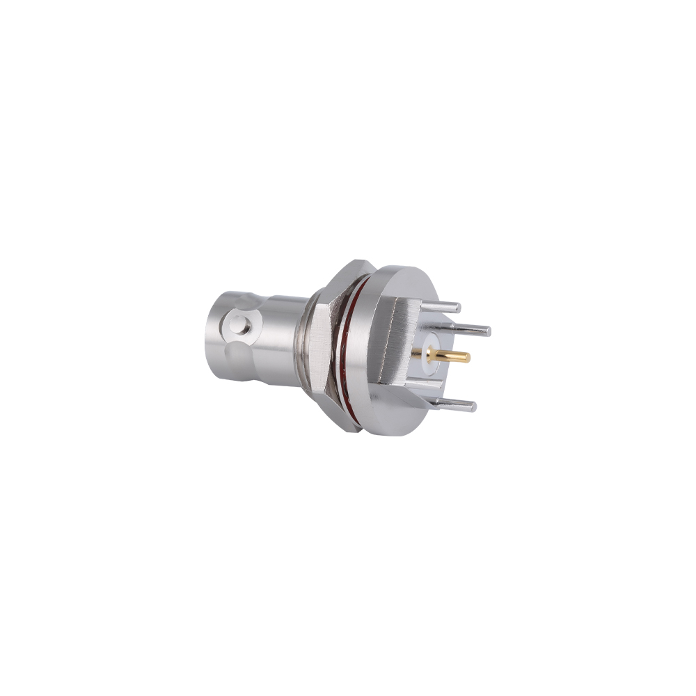
The BNC PCB (Printed Circuit Board) Connectors are directly mounted to the PCB surface or through-hole plated vias, eliminating the need for a separate cable pigtail between the board and the connector. This integration reduces assembly steps, minimizes parasitic inductance/capacitance from intermediate cable transitions, and frees up space inside the product enclosure.
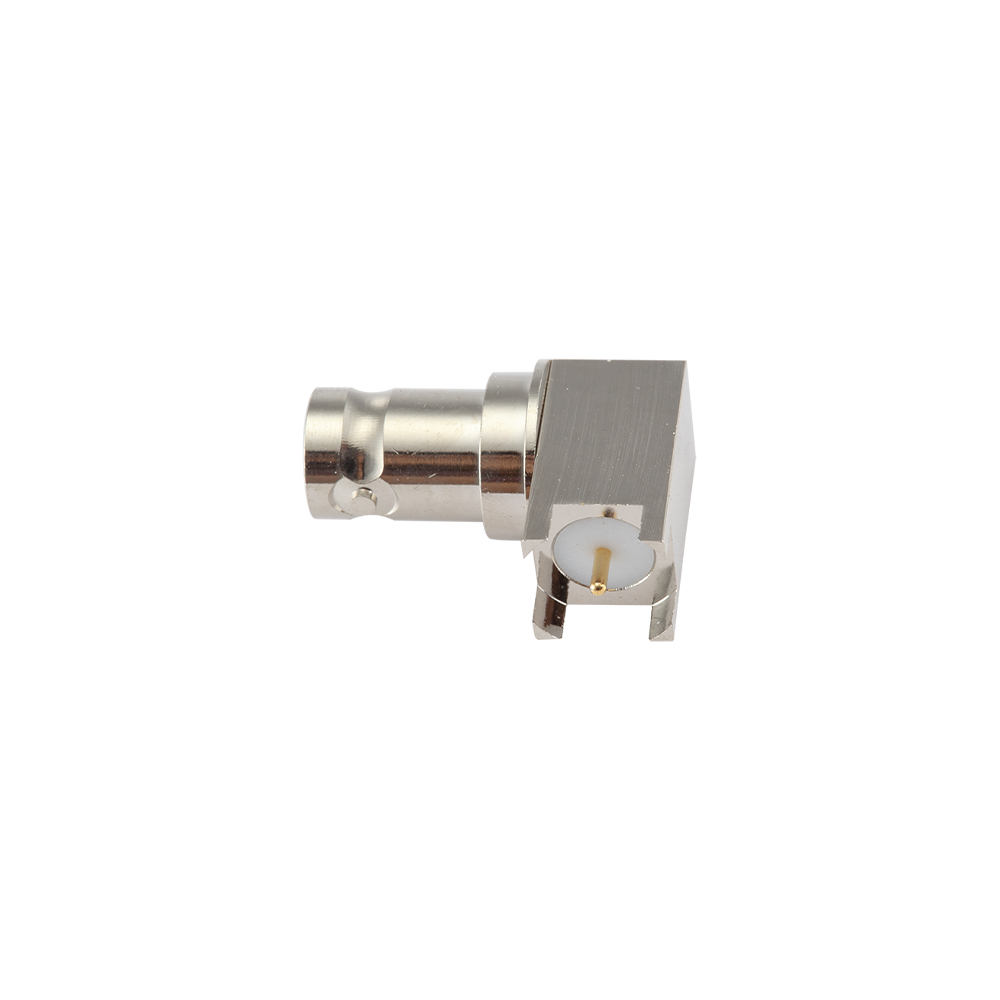
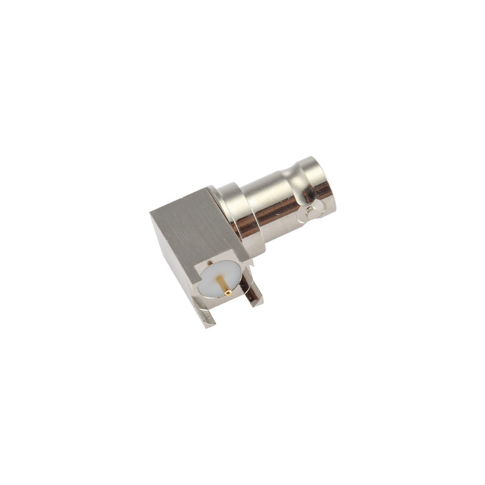
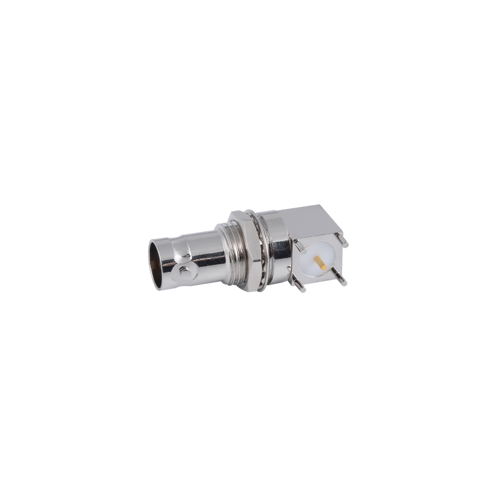
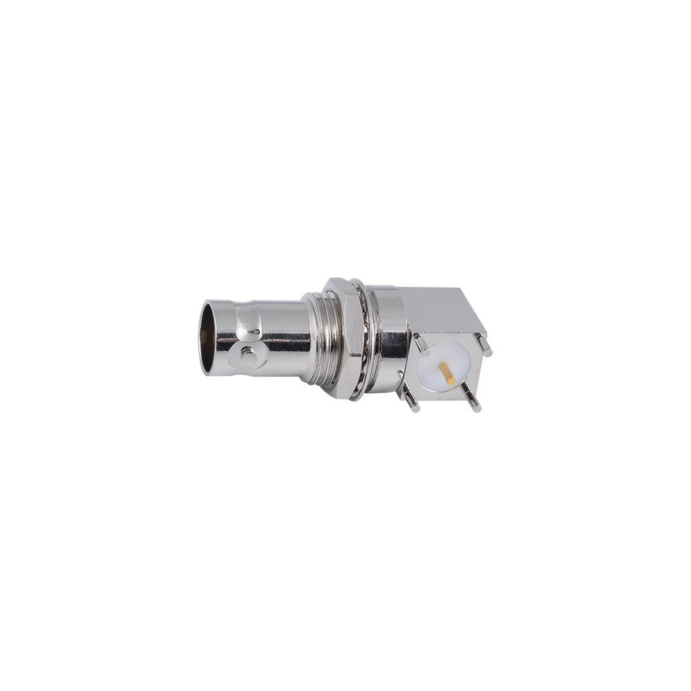
PCB-mount BNC connectors appear at the edge or interior of the PCB, either as right-angle (edge-launch) types that extend horizontally off the board edge to mate with panel-exit cables, or as vertical (top-launch) types that mate perpendicular to the board plane. Both configurations are engineered to maintain impedance integrity through the PCB transition, which is critical for high-frequency signal integrity.
Key Features
Through-hole and surface-mount (SMT) attachment options: through-hole pin styles for mechanical robustness in high-vibration environments; SMT footprints for reflow-solderable automated PCB assembly lines.
Right-angle (horizontal) and vertical (upright) PCB mount orientations available, providing layout flexibility for both edge-mount and center-board placement.
Controlled impedance center pin and dielectric geometry maintains 50Ω or 75Ω impedance through the PCB launch transition, preserving signal integrity to the board layer stack.
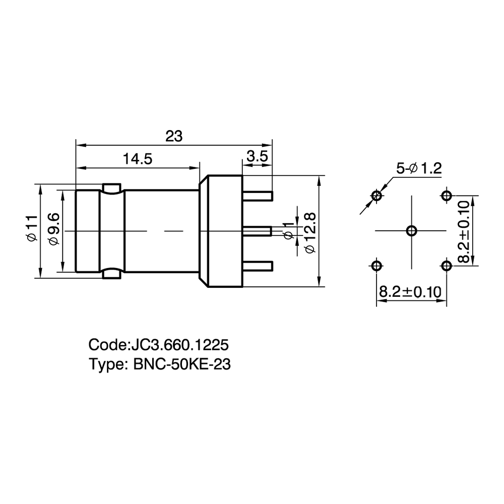
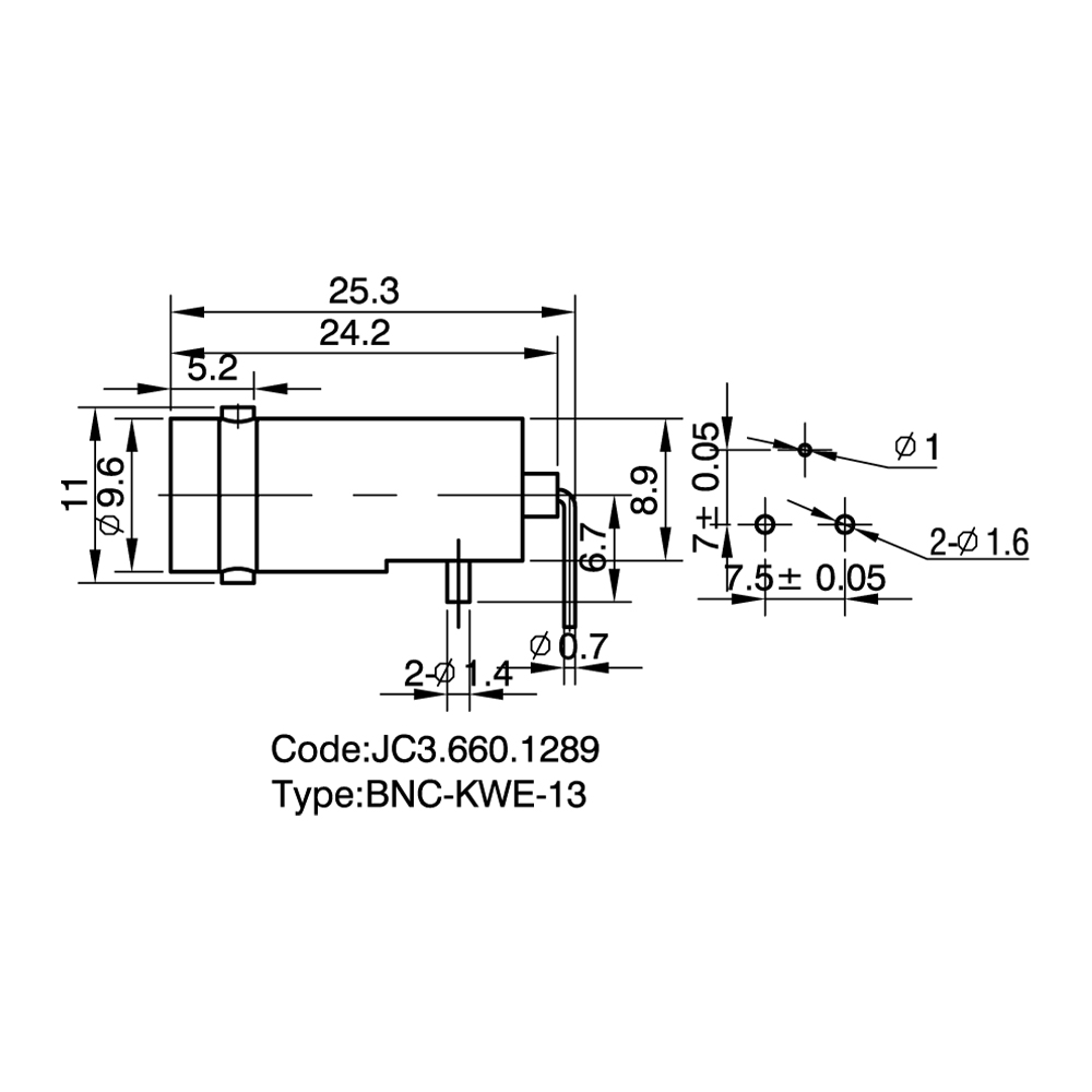
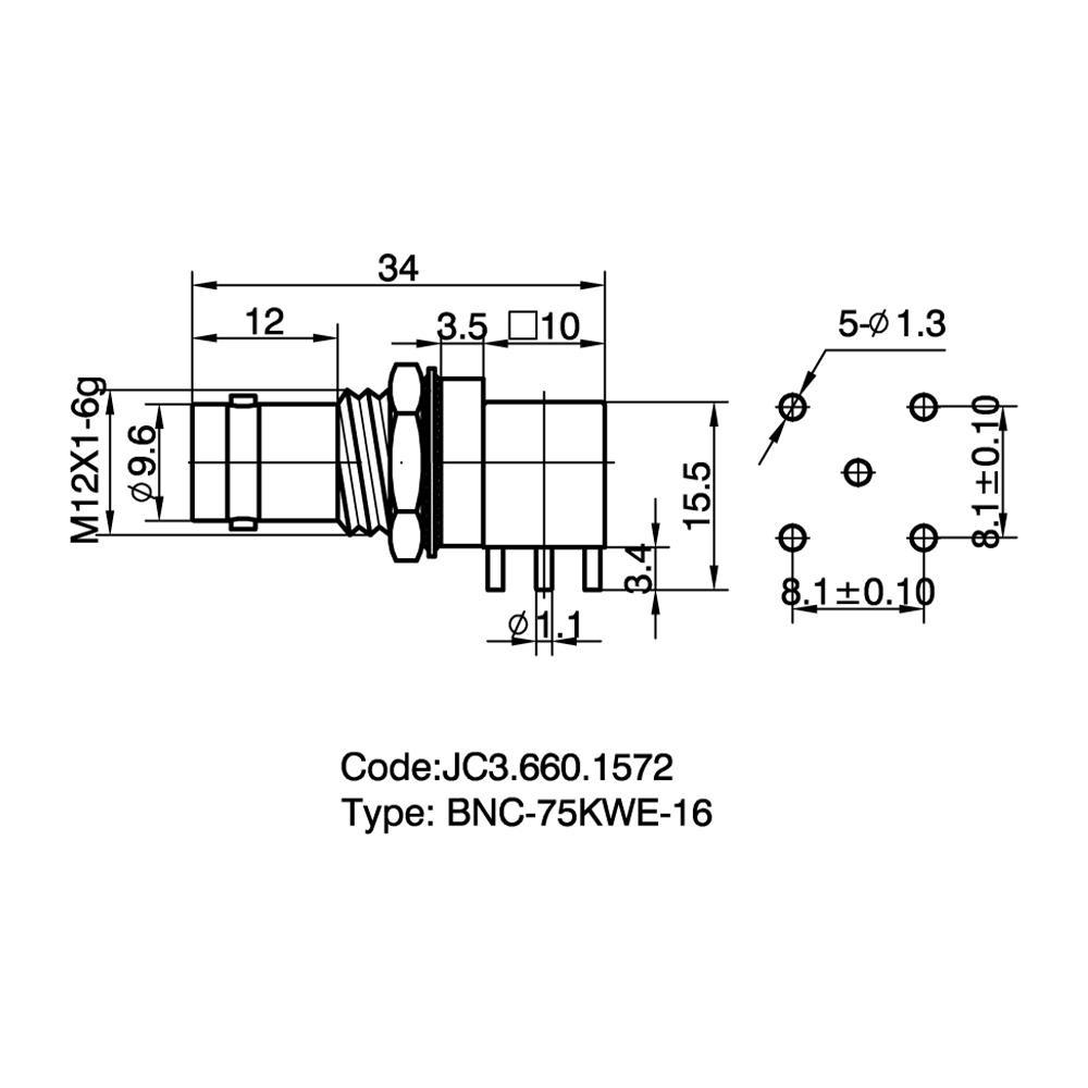
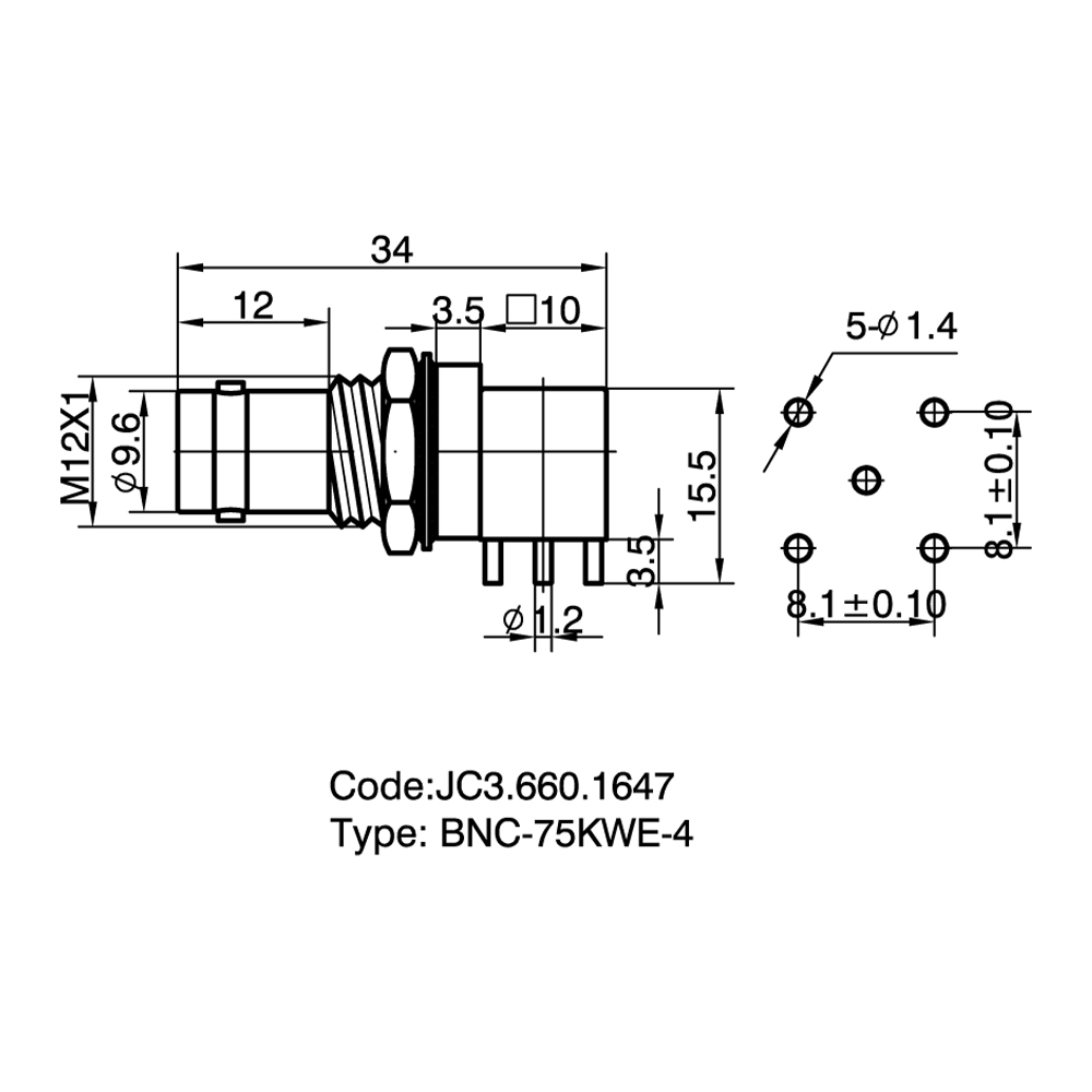
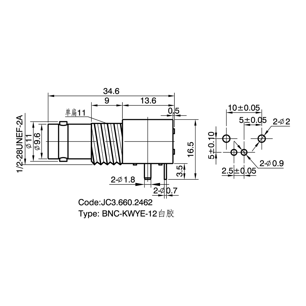
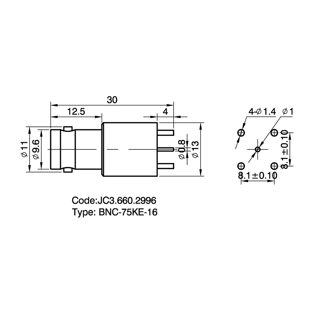
PCB-compatible solder tail geometry with industry-standard land pattern dimensions; Gerber footprint data available on request to accelerate PCB layout.
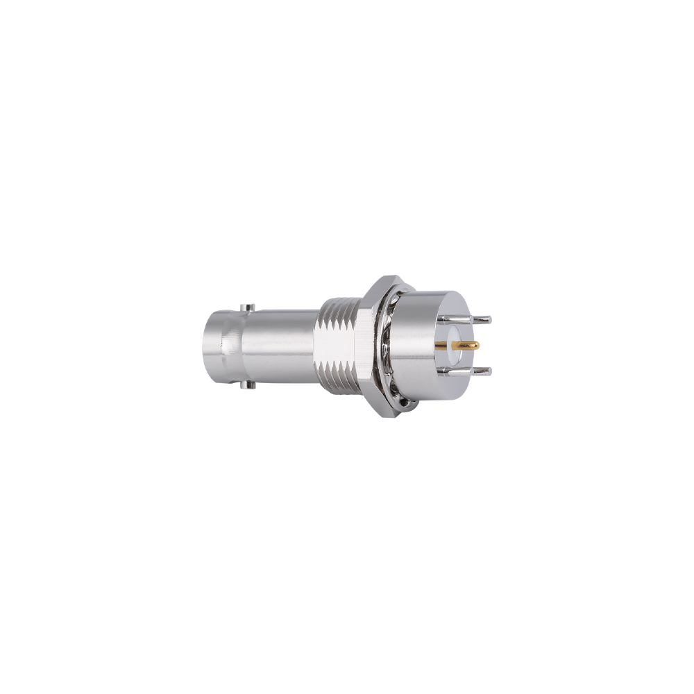
Flange-mount PCB versions with additional solder tails or screws provide mechanical anchoring to resist cable pull forces that would otherwise stress solder joints.
Operating frequency to 4GHz covers the full BNC-defined band; some selected variants extend performance further for applications approaching this upper limit.
Competitive Advantages
As an R&D-driven manufacturer with its own engineering technology research center, Jingcheng can support customer PCB layout reviews, providing impedance transition analysis and recommendations to minimize signal reflection at the board launch point—a value-added service rarely offered by pure-trading connector companies.
Product conformance to IEC 169-8 ensures that equipment assembled with Jingcheng PCB BNC connectors passes BNC interface-level interoperability testing with any compliant mating connector, simplifying system integration for OEM customers.
SMT reel packaging available for high-volume PCB assembly line integration; tape-and-reel dimensions and component orientation data provided with the part datasheet.
Lead-free (RoHS) solder-compatible finishes as standard, with full material declarations (IPC-1752) available to support product environmental compliance documentation.
Typical Applications
RF PCBs in wireless communication modules (WiFi, Bluetooth, Zigbee, sub-GHz ISM band)
Test and measurement PCB assemblies requiring front-panel BNC jacks hard-mounted to the board
Industrial IoT sensor boards with direct antenna or cable connections
Medical device PCBs for patient telemetry and physiological monitoring modules
SDR (Software Defined Radio) development boards and prototype RF platforms
Automotive telematics control units requiring compact RF board-edge connectors
FAQ
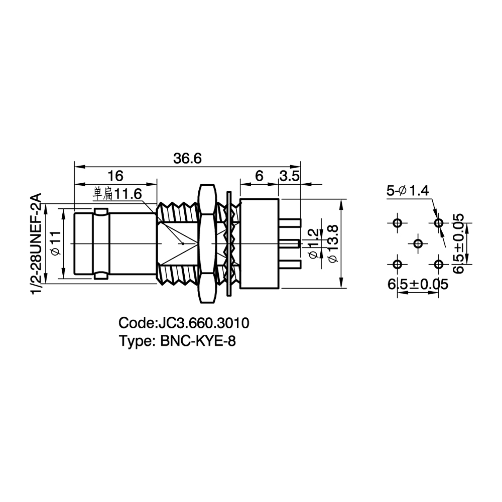
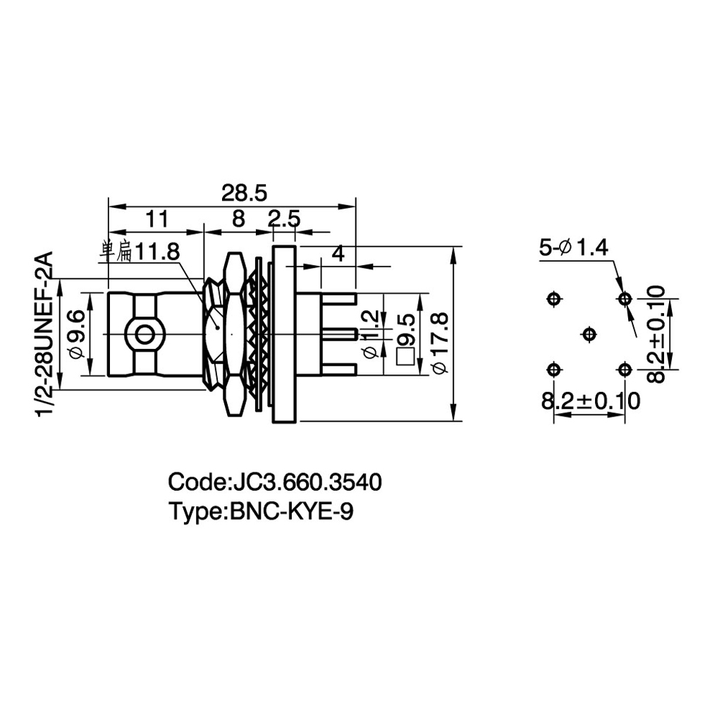
Q: Are IPC-compatible land pattern drawings and 3D STEP models available for the PCB connectors?
A: Yes. Dimensional drawings and 2D land pattern data are provided with product datasheets. 3D STEP models are available for standard catalogue variants upon written request, typically delivered within 5 business days.
Q: What PCB thickness range is supported by the through-hole variants?
A: Standard PCB through-hole tail lengths are designed for 1.6mm (standard) and 2.4mm PCB thicknesses. Custom tail lengths for other PCB thicknesses (e.g., 3.2mm for power/RF combined boards) can be quoted as engineering specials.
Q: Can the SMT version be soldered in a standard lead-free reflow profile?
A: Yes. All SMT PCB connector variants are designed for standard IPC/JEDEC lead-free reflow profiles (peak temperature 260°C). The PTFE or high-temperature thermoplastic dielectric materials used maintain dimensional stability through the reflow cycle without voiding or delamination.
Q: Is there a right-angle PCB connector with a latching mechanism for secure mating?
A: Standard BNC connectors use the quarter-turn bayonet locking mechanism, which is consistent across all variants including PCB-mount versions. This provides secure mating with tactile engagement confirmation. Alternative retention mechanisms are not standard in the BNC series by IEC specification.
Q: What distinguishes Jingcheng BNC PCB connectors from lower-cost alternatives on the market?
A: The primary differentiators are dimensional precision (controlled by Hanwha CNC machines), plating consistency (monitored through in-house electroplating), and electrical validation (using Agilent network analyzers). These process controls, backed by ISO9001 and GJB9001A certification, deliver connector lots with consistent insertion loss and VSWR across the full production run—not just on the qualification samples.
|
Temperature Range
|
-55~+155℃ (PE Cable -40~+85℃)
|
|
Impedance
|
50Ω, 75Ω
|
|
Frequency Range
|
DC~4GHz
|
|
Insulation Resistance
|
≥5000MΩ
|
|
Insertion Loss
|
≤0.20 dB/1GHz
|
|
VSWR
|
Straight ≤1.22/3GHz Right angle ≤1.30/3GHz
|
|
Durability(mating)
|
≥500 (cycles)
|